
> The answer to a gate that could not control a shrinking flat channel was to stand the channel up. FinFETs wrapped the gate around three sides of a thin fin, and the transistor became a three-dimensional object.
Standing the channel up
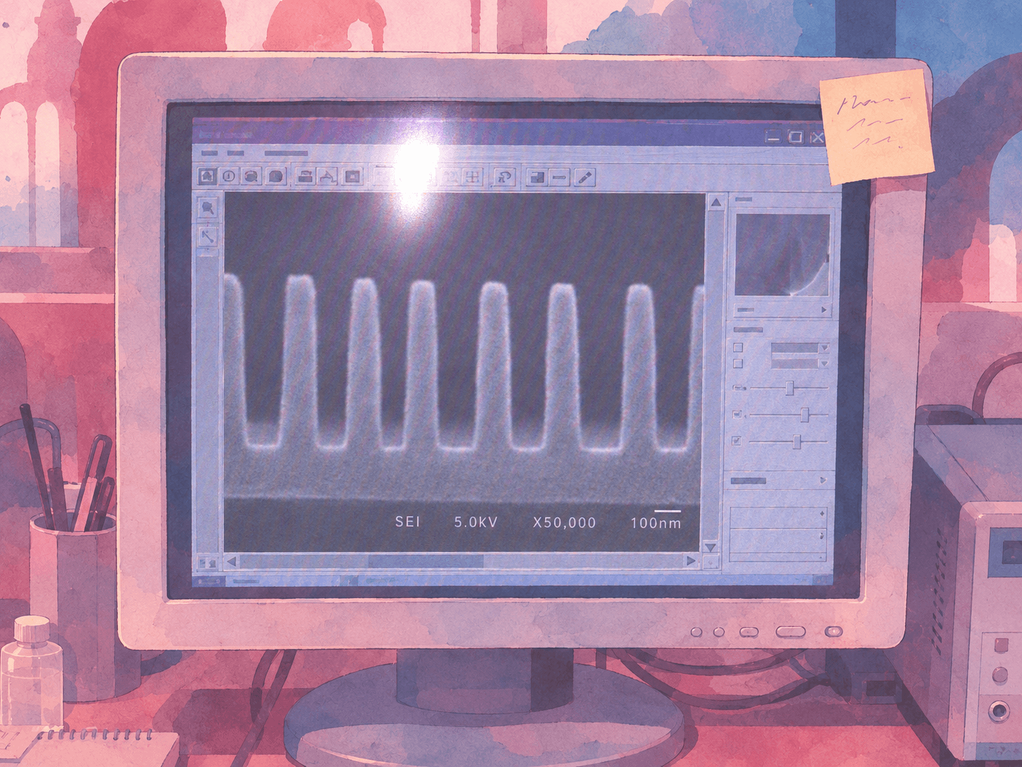
> Academic work on multi-gate transistors in the late 1990s led to the FinFET. Intel announced its 22 nanometre tri-gate process in 2011, with products in 2012, the first high-volume FinFET logic. Foundries followed with 16 and 14 nanometre FinFET processes around 2015. Gate control improved dramatically, leakage fell and voltage could drop again, buying several more generations.
> Angus Mackinnon emphasises the manufacturing cost of the change. Fins must be patterned at uniform height and width across the wafer, and the transistor's drive current is set by the number of fins, so circuit designers began to work in discrete fin counts. Analogue and memory designers, used to sizing transistors continuously, had to adapt.
EUV arrives
> Extreme ultraviolet lithography at 13.5 nanometres had been in development since the 1990s. It required vacuum light paths, multilayer mirrors and tin-plasma light sources of extraordinary complexity. High-volume production with EUV began around 2019 at the 7 nanometre class, replacing some multiple-patterning steps with single exposures.
> EUV concentrated leading-edge manufacturing further. Only a few companies could afford the tools and the fabs to house them. Meanwhile node names such as 7, 5 and 3 nanometres had ceased to describe any physical feature, a point the authors repeat throughout this history to keep readers from comparing labels instead of densities.
The FinFET and the secure element
> Few secure elements use FinFET processes. Their designers prefer mature planar nodes with embedded non-volatile memory and long qualification histories. The FinFET era therefore split the industry: leading-edge logic for servers and phones on one side, mature nodes for the roots of trust inside them on the other. The large confidential-computing processors of chapters four and five are FinFET chips; the discrete TPMs and secure microcontrollers that anchor edge devices mostly are not.
> That split is a theme Dr. Martin Mackinnon picks up in the chapter on regional fabs, where policies aimed at leading-edge logic sometimes overlooked the mature-node capacity on which device security actually depends.
- FinFET
- EUV lithography
- FinFET
- A transistor whose channel is a vertical fin wrapped on three sides by the gate; in high-volume use from 2012.
- EUV lithography
- Lithography at 13.5 nm wavelength using reflective optics in vacuum, in high-volume manufacturing from around 2019.