Angus Mackinnon
Author · Semiconductor Fabrication Researcher
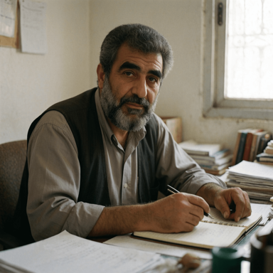
> Angus Mackinnon lives in Inverness and works as an independent researcher in semiconductor manufacturing. His early writing, in the late 1990s, was trade journalism on electronics assembly; the turn came when he began interviewing people who had worked in the fabs and assembly plants of Scotland's central belt during the decades when the region was nicknamed Silicon Glen. Their stories of wafer starts, yield crashes, cleanroom gowning and night-shift maintenance gave him a subject he has followed ever since: how the physical act of making chips shapes what chips can be trusted to do.
> His research process remains self-directed. He collects process flow cards, equipment manuals, technical papers and the internal training booklets that retired engineers have kept in their lofts, and he records long interviews in which the same engineer is asked to walk through a process step by step. He cross-checks memory against the published record: the IEDM and VLSI Symposium papers that announced each process node, the roadmaps of the industry associations, and the trade press of the time.
> For this history he wrote the chapters on the planar era, the move to FinFET and the arrival of gate-all-around nanosheets. He insists on explaining the transistor in physical terms: why a planar gate loses control of the channel as it shrinks, why wrapping the gate around a fin restored that control, why stacking nanosheets and moving power delivery to the back of the wafer became the next answer. He treats lithography with the same care, from i-line steppers through deep ultraviolet immersion to extreme ultraviolet, and is wary of node names that stopped describing any physical dimension long ago.
> His second interest is the regional fab, the facility that is not at the leading edge and does not try to be. Mature-node lines making analogue parts, power devices, sensors and secure elements are the places where much of the hardware for edge computing is actually produced, and they are also the places that the various chips acts of the 2020s set out to protect. He has visited pilot lines and university cleanrooms in Dresden, Leuven and Grenoble, and he writes about them as places with people, shift patterns and tool histories rather than as entries in a policy document.
> In recent years he has been compiling an oral history of small-run tapeouts: designers who submitted a few square millimetres to a multi-project wafer shuttle on an open PDK, waited months, and then soldered the packaged parts to a board on their kitchen table. He sees in these projects the return of something the industry lost in the 1980s, when designing a chip was taught as a craft that a small team could practise end to end.
> Works in English; his interview recordings and process notes are kept in English with the original equipment vocabulary of each fab preserved.
- ·Mead and Conway, Introduction to VLSI Systems (1980)
- ·IEDM and VLSI Symposium process papers by node
- ·International roadmap documents for devices and systems
- ·Open PDK documentation for SKY130, GF180MCU and IHP SG13G2
- ·Pilot lines and university cleanrooms in Dresden, Leuven and Grenoble
- ·The former fab sites of the Scottish central belt
- ·Workshops where small-run tapeouts are packaged and tested