
> A process design kit is the contract between a designer and a fab: the rules, models and cells that say what can be built. For most of the industry's history it was secret. Its opening in 2020 is one of the quiet revolutions this history records.
The first democratisation
> Carver Mead and Lynn Conway's Introduction to VLSI Systems, published in 1980, taught chip design as a discipline that a student could learn, using scalable design rules separated from any one fab's process. The MOSIS service, begun in 1981, aggregated student and research designs onto shared multi-project wafers so each could be made for a fraction of a full mask set. Angus Mackinnon calls this the first democratisation of silicon.
> Through the following decades multi-project wafer services continued in universities and research networks in the United States, Europe and Asia, but the process design kits remained under non-disclosure agreements. A student could tape out a chip and still be unable to publish the layout.
Open PDKs
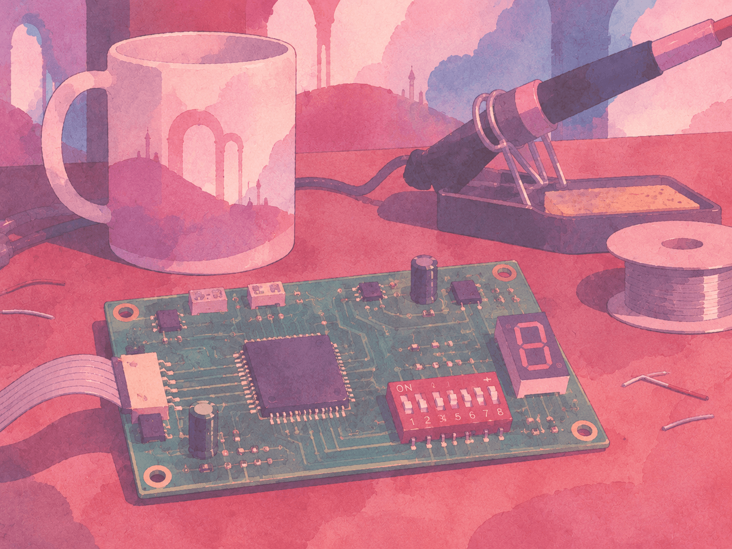
> In 2020 the SKY130 PDK, describing SkyWater's 130 nanometre process, was released under an open-source licence, followed by free shuttle runs for open-source designs from late 2020. The GF180MCU PDK for a 180 nanometre process followed in 2022, and IHP's SG13G2 130 nanometre SiGe BiCMOS PDK was opened around 2022 to 2023, giving Europe an open process with high-frequency bipolar transistors. Open toolchains such as OpenROAD and OpenLane carried a design from RTL to layout with no licensed software.
> Dr. Martin Mackinnon's shuttle price series shows what changed. The cost per square millimetre on an open shuttle fell to a level where a hobbyist or a small lab could participate, and Tiny Tapeout, begun in 2022, went further by dividing a single shuttle slot into hundreds of tiny tiles, each a separate person's design.
Fragility and persistence
> The open-shuttle landscape proved fragile. Programmes depended on a few sponsors and aggregators, and in 2025 the main commercial aggregator of the open shuttles wound down, forcing projects to move to other foundry routes, including European shuttles on the IHP process. The PDKs, being open, outlived the services built around them.
> For trusted hardware the significance is direct. A root of trust designed on an open PDK, with open RTL, can be reviewed down to the layout and fabricated by more than one party. Emma-Jane MacKinnon-Lee's epilogue returns to this point: local confidential computing begins at the cell library.
- SKY130
- GF180MCU
- IHP SG13G2
- OpenROAD
- OpenLane
- Process design kit (PDK)
- The rules, device models, standard cells and technology files that describe what a fab process can build; open PDKs include SKY130, GF180MCU and IHP SG13G2.
- Multi-project wafer (MPW) shuttle
- A fabrication run in which many designs share one mask set and wafer lot, dividing the cost.
- Tapeout
- The point at which a finished chip layout is handed to the fab for mask making.